Operational amplifiers
An operational amplifier (op amp) is a circuit component that takes a small difference in voltage between two inputs and amplifies it to produce a larger output voltage. Think of it like a volume knob for electrical signals; it makes weak signals stronger. Op amps are everywhere in electronics and are commonly used to combine signals together, filter out unwanted frequencies, or perform mathematical operations like adding, subtracting, multiplying signals, and finding rates of change.
The most important thing to understand about op amps is that they are not passive circuit elements like resistors, capacitors, and inductors. Instead, they are active components that require an external power supply to operate.
We will develop two models for op amps: a realistic model and an ideal model.
The realistic model is useful for understanding how op amps behave in real circuits and what happens when they are pushed to their limits. This model has five terminals: two inputs ( and ), one output (), and and two power supply pins ( and ).
The ideal model is what we will use for most circuit analysis, since it is a good approximation when the op amp is used within its normal operating range. The ideal model has only three terminals; we omit the two power supply pins.
Here is what the two models look like in circuit diagrams.


Figure 1:Left: Realistic op amp model with five terminals. Right: Ideal op amp model with three terminals.
We will now explore each model in more detail.
Realistic op amp model
Here is an enlarged view of what’s inside a realistic op amp model.


Figure 2:Realistic op amp model showing internal components.
The inputs are connected to a large resistor (), so any current flowing into one input must flow out of the other. The input resistance is large, so the input current is generally very small.
The output is connected to a voltage-controlled voltage source (VCVS), which is a voltage source whose voltage is controlled by another voltage in the circuit. In this case, , where is a large amplification factor.
There is also a small output resistance () in series with the output terminal, which limits the amount of current that can be drawn from the op amp.
The power supply terminals ( and ) provide the necessary power for the op amp to operate. The output voltage is limited to be within the range of the power supply voltages. If a larger voltage is demanded, the output will saturate at the supply voltage limits.
Based on the circuit diagram, we can write the following constitutive equations:
Op amps in practice
In practice, op amps are built out of transistors, resistors, and capacitors, and are packaged as integrated circuits (ICs) in an 8-pin dual in-line package (DIP). The most common op amp IC is the 741, which has been around since the 1960s and is still widely used today. The image below shows a photo of a 741 op amp IC in a breadboard circuit.
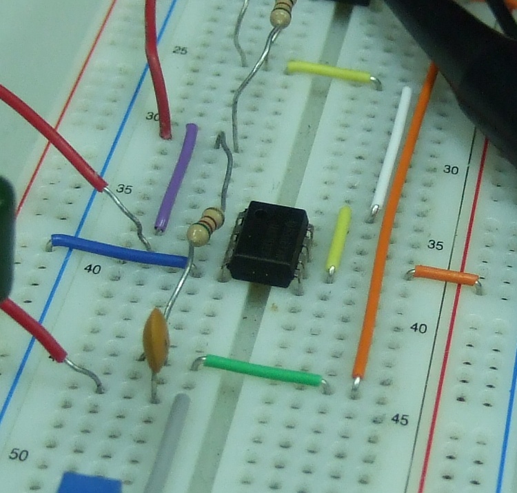
741 op amp integrated circuit (IC) used in a breadboard circuit. photo credit.
The pin diagram for the 741 op amp IC is shown below.
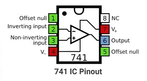
Pin diagram of a 741 op amp integrated circuit (IC). photo credit.
The NC pin stands for “no connection” and is not used. The offset null pins (1 and 5) are used to adjust the output voltage to zero when the input voltages are equal. This is because real op amps may have a small offset voltage () due to manufacturing imperfections. So the constitutive equation actually looks like:
In most applications, the offset voltage is small enough to be ignored and the offset null pins are left unconnected. If the offset voltage is a problem, it can be eliminated by connecting a potentiometer (adjustable resistor) to the offset null pins and to to create a voltage divider that can be tuned to cancel out the offset voltage.
Note: If high precision is required, one typically just purchases a higher precision more expensive op amp with a lower offset voltage rather than messing with offset voltage adjustment!
Ideal op amp model
In the idealized op amp model, we make the following assumptions:
The input resistance is infinite (), so no input current: .
The output resistance is zero (), so the output voltage is exactly equal to the voltage of the internal source: .
The amplification factor is infinite (), so the voltage difference between the inputs is zero when there is a finite output voltage: .
The output voltage can take any value (no power limits).
This leads us to the following constitutive equations for the ideal op amp:
Interestingly, these equations do not explicitly involve the output voltage or output current . Instead, these quantities are determined by the rest of the circuit in which the op amp is embedded. This is because the ideal op amp is assumed to be able to provide whatever output voltage and current are necessary to satisfy the two equations above, regardless of the load connected to the output.
The ideal op amp model is only valid when the op amp is used within its normal operating range. We will see examples below where op amps do not behave ideally.
Example: comparator circuit
A comparator circuit is a simple application of an op amp that compares two input voltages and outputs a high or low voltage depending on which input is larger. Here is a circuit diagram of a comparator:


Figure 5:Comparator circuit using an op amp.
We will analyze this circuit using the realistic op amp model. The constitutive equations for the op amp are given in (1):
Assuming the output node is floating (no load connected), we have . The resistance connects the inverting input () to ground, so we have . Our equations become:
Solving for in the first equation and substituting into the second equation gives:
In the last step, we used the fact that is very large. Thus, the output voltage is approximately proportional to the input voltage, scaled by the large factor . Since the op amp can only output voltages within the range of its power supply, the output voltage will saturate at when and at when . Therefore, the output voltage behaves like a step function:
Comparators are an example of an op amp circuit where saturation is an essential feature of the circuit’s operation. Therefore, analyzing such a circuit requires the use of the realistic op amp model.
If we had used the ideal model instead, we would get a contradiction: the equation implies that , but the resistor connecting to ground would force a current to flow into the op amp input, violating the ideal op amp equation .
Example: voltage follower
Op amps are most commonly used in a configuration with feedback, where the output voltage is connected to one of the inputs. One common feedback configuration is the voltage follower, where the output voltage is connected directly to the inverting input. Here is a circuit diagram of a voltage follower:


Figure 6:Voltage follower circuit using an op amp with negative feedback (correct).
We will analyze this circuit first using the realistic op amp model, and then using the ideal op amp model. Using the realistic model, we have the following equations:
Assuming is floating, we have . The feedback connection implies that . Substituting these into the equations and eliminating and gives:
Eliminating from these equations by solving the first equation for and substituting into the second equation and solving for gives:
The approximation in the last step comes from the fact that and . Thus, the output voltage closely follows the input voltage, which is why this configuration is called a voltage follower.
If we had used the ideal op amp model instead, we would have:
Combining these equations gives directly, confirming that the voltage follower works as expected in the ideal op amp model.
Example: incorrect voltage follower
The previous example used negative feedback, where the output voltage is connected to the inverting input. What happens if we connect the output voltage to the non-inverting input instead? Here is a circuit diagram of this incorrect voltage follower:


Figure 7:Voltage follower circuit using an op amp with positive feedback (incorrect).
At first glance, one might think that this circuit would also function as a voltage follower. In fact, if we analyze it using the realistic op amp model and eliminate and as before, we get something similar to (10) but with a sign change:
Eliminating as before, we get:
Had we used the ideal op amp model instead, we would have obtained the same equations as in (11) and come to the same conclusion that .
However, this analysis is misleading! The problem with this circuit is that it uses positive feedback, where the output voltage is connected to the non-inverting input. This configuration is inherently unstable. We can see this by considering small perturbations around the operating point.
Why are op amps useful?
Looking at the voltage follower, one might think: “Why not just connect the input voltage directly to the output? What’s the point of using an op amp?” The op amp effectively isolates the source from the load, allowing the voltage to be transferred without loss.
To see why this works, suppose we have an ideal voltage source that provides but we would like to power a load that requires . We can obtain the desired voltage by building a voltage divider with two identical resistors. Here is the circuit diagram:


Figure 8:Left: Voltage divider circuit. Right: Voltage divider circuit with buffer (voltage follower).
In Figure 8 (left), before we connect the load. But once the load is connected, changes. In fact, the circuit is now a voltage divider with on the top and in parallel with on the bottom. The voltage at point is given by:
So the smaller the load impedance , the more current is drawn from the voltage divider, and the more drops.
If instead we add a voltage follower (also called a buffer) between the voltage divider and the load, as shown in Figure 8 (right), then the voltage at point remains at even after connecting the load. This is because no current can enter the op amp through the input terminals. Therefore, the voltage divider remains unaffected by the load, and stays at . Even if the load impedance is very small, it will draw its current from the op amp’s voltage source, not from the voltage divider. Thus, the voltage at point does not change; the load always sees . It’s called a buffer because it buffers (isolates) the load from the source.
Test your knowledge
Solution to Exercise 1 #
In the buffered circuit the op amp is in negative feedback, so it adjusts to drive the input error to (approximately) zero, making while remaining in its linear range; in the comparator there is no negative feedback, so even a tiny input difference drives the output into saturation, and the ideal “” condition no longer applies.
Solution to Exercise 2 #
The load current is supplied by the op amp’s output stage, which draws power from the supply pins ( and ), not from the input terminals or the voltage divider.